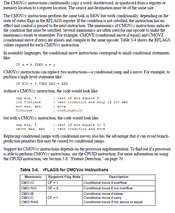
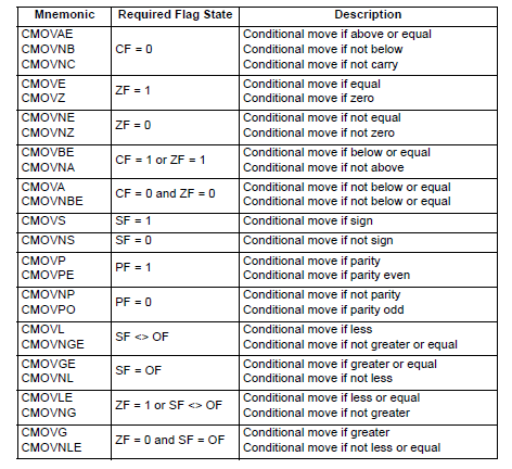
UNDER CONSTRUCTION
0 0000
1 0001
2 0010
3 0011
4 0100
5 0101
6 0110
7 0111
8 1000
9 1001
a 1010
b 1011
c 1100
d 1101
e 1110
f 1111
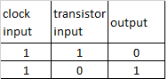
A Transistor is a switch that can be ON or OFF.
an open transistor, therefore without contact between the conductors, is not crossed by electricity, provides the binary number = 0
while a closed transistor, then with contact between conductors, is traversed by current, provides the binary number = 1
The Intel pentium4 microchip has over 43,000,000 transistors, AMD athlon has at least 37,000,000.
The Oscillator, ie the Clock, adjusts the working speed of the computer, more beats = greater speed, measured in megahertz,
i.e millions of beats per second.
the current passing through a transistor can be used to control another transistor. It turns the switch on ON or OFF
to change the status of the second transistor. This configuration is called PORT.
the logic port NOT is composed of a single transistor that takes an Input from the Clock and an Input from another transistor.
this Port produces only one output, which is always the opposite of the input coming from the transistor
different combinations of NOT ports create other logical ports
OR 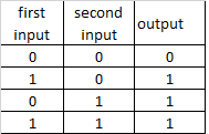
AND 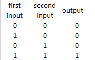
XOR 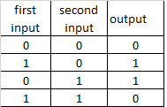
using different combinations of logical ports , the microchip executes the Addition operation from which
all other mathematical operations descend.
the addition is executed through structures called Half-Adder and Full-Adder
a half-adder is made by a port XOR and a port AND which receives both the same Bit in input
eg:
2d + 3d = 10b + 11b
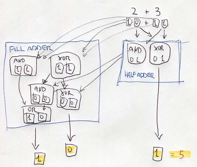
half-adder processes the digits at right using the portd XOR and AND
the resutl of XOR is the digit at right of the final result
the result of AND is the input of ports XOR and AND of the full-adder
also, the full-adder processes the digits at left of thr bits 10 and 10
the results are the inputs of other ports AND and XOR
the results are processed with the results of the half-adder
one of these results is the input of OR
all the results gives the binary number 101 that is 5 on decimal numbers
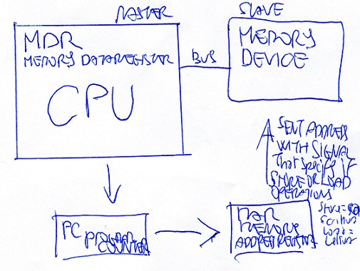
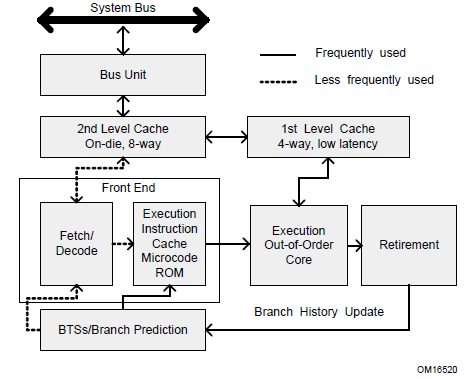
MC includes (CPU=MP) + ((cache level 2 (greater and faster than cache level 1 included in MP))
BIOS = SW normally contained in ROM or other non-volatile memory, beetween HW and SW
Clock - clock frequency - is the number of switches 0 and 1 that circuits in MP, normally
an instruction needs of more clock cycles.
Quartz Oscillator which is inside the cpu=mp and can be controlled via BIOS
CMOS complementary metal-oxide semiconductor, microchips that maintains hardware and
configuration settings by the power of a buffer battery
ENDIAN
In big endian, you store the most significant byte in the smallest address.
In little endian, you store the least significant byte in the smallest address.
Real Mode can use 1MB of segmented memory address only. all CPU so started (initially the bus had 20 bit of addresses
Protected Mode, CPU begins executing instructions in real mode, then can use the virtual memory and the multitasking
Buffer - transit memory or even intermediary memory area used to compensate for differences
in speed in the transfer or transmission of data, or to speed up execution of some operations
such as operations on character strings.
cache level 1 (I-cache = instruction cache + D-cahe = data cache) is inside MP
cache level 2 , greater and faster than L1, is in MC but extern and near at MP
BIU bus interface unit , input of info in processor, duplicates infos and send to
cache L1 (I-cache and D-cache) and to Cache L2
Fetch decode unit , fetches instructions from I-Cache ,
BTB branch target Buffer, compares every instruction with a record of another buffer
to verify if this instruction already is already used
A batch file is a script file in DOS, OS/2 and Microsoft Windows. It consists of a series of commands to be executed by the command-line interpreter,
stored in a plain text file. When a batch file is run, the shell program (usually COMMAND.COM or cmd.exe) reads the file and executes its commands,
normally line-by-line. Unix-like operating systems, such as Linux, have a similar, but more flexible, type of file called a shell script.
When DOS loads, the file AUTOEXEC.BAT, when present, is automatically executed, so any commands that need to be run to set up the DOS environment
may be placed in this file. Computer users would have the AUTOEXEC.BAT file set up the system date and time, initialize the DOS environment,
load any resident programs or device drivers, or initialize network connections and assignments.
.bat
file name extension identifies a file containing commands that are executed by the command interpreter COMMAND.COM line by line,
the first filename extension used by Microsoft for batch files.
.cmd
Used for batch files in Windows NT family and sent to cmd.exe for interpretation. COMMAND.COM does not recognize this file name extension, so cmd.exe scripts
are not executed in the wrong Windows environment by mistake. In addition, append, dpath, ftype, set, path, assoc and prompt commands, when executed
from a .bat file, alter the value of the errorlevel variable only upon an error, whereas from within a .cmd file, they would affect errorlevel even when
returning without an error.[3] It is also used by IBM's OS/2 for batch files.
.btm
The extension used by 4DOS, 4OS2, 4NT and Take Command. These scripts are faster, especially with longer ones, as the script is loaded entirely
ready for execution, rather than line-by-line.
Segment+Offset 
Segment registers and Offset (instruction pointer register) have still 16 bits.
Program Counter (physical address) = CS:IP = code segment*16 to have 20 bits + Instruction Pointer (EA effective address)
BTB Branch Target Buffer
In the microprocessor architecture the target predictor branch is a functional unit dedicated to prediction
of the arrival address of a conditioned branch or an unconditional jump before the instruction was
loaded from the instruction cache. The instruction cache is a specialized cache.
The target predictor branch should not be confused with the branch prediction unit as this unit looks for
predicting whether the branch will be followed or not.
In many parallel processors the instruction cache has a relatively high latency and therefore the identification of the address
of arrival of the jump represents a bottleneck. The procedure for its identification carries out the following
operations:
The instruction cache provides a block of instructions
The instruction block is analyzed in the branch search
The branch prediction unit identifies the first jump that should be performed
The jump destination address is calculated
Instructions are loaded from that address
In many processors these operations require two clock cycles and therefore the processor loses a complete clock cycle
to load the new instructions after each predicted jump. Given that on average a predicted jump is present every ten
instructions performed the loss of performance can be significant. Some processors have high latency
cache instructions and therefore the performance degradation is even higher. To reduce the performance loss many
processors include a target predictor branch unit, given the address of the jump this unit predicts the destination of the
jump. An improvement of the idea predicts the beginning of sequential instructions starting from the address of the previous block
of sequential instructions.
Prediction reduces the operations to be performed which become:
Hash of the address of the first sequential instruction
Loading from the predictor of the address of the jumps present in the block of instructions in execution
Selection of the arrival address of the first predicted jump
The predictor occupies about 5-10% of the instruction cache space but the loading of the instructions after the jump is
speeded up considerably. If it were not fast enough you could parallelize the prediction of the addresses of the
jumps and prediction of jumps.
The prediction percentage of a jump is around 93% of successes.
PIPELINE is a set of data processing elements connected in series,
where the output of one element is the input of the next one.
The elements of a pipeline are often executed in parallel or
in time-sliced mode.
Some amount of buffer storage is often inserted between
elements. Pipelines include:
Instruction pipelines, such as the classic RISC pipeline,
which are used in central processing units (CPUs) and
other microprocessors to allow overlapping execution of
multiple instructions with the same circuitry.
The circuitry is usually divided by stages and each
stage processes a specific part of one instruction at a time,
passing the partial results to the next stage.
Examples of stages are instruction decode,
arithmetic/logic and register fetch. They are related to
the technologies of superscalar execution, operand forwarding,
speculative execution and out-of-order execution.
address of 1st element of SP = FFFEh
element size = W = 2B
Stack overflow (overwritten memory locations of program, but not of the OS) indefinite filling of Stack
Heap area = Dynamic Memory = optional zone, where during runtime, the programmer, through instructions,
temporarily allocates some memory for variables whose dimension can only be verified
during execution (eg the size of an input string). Its size is not predetermined and
can also be allocated and deallocated several times during runtime.
The management of the area of heap is obtained through code area instructions.
Stack area = memory zone handled automatically by Compilers. By programmer instructions
the compilers manage the area of stack transparently to the programmer,
allocating and deallocating the local variables and parameters passed to the procedures.
Only in the Programming in Assembly it's possible directly handle the stack area
with appropriate instructions.
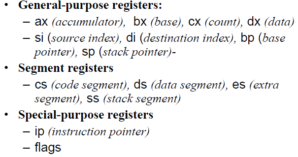
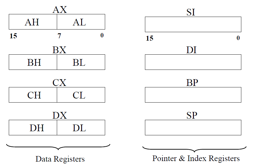
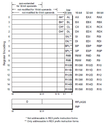
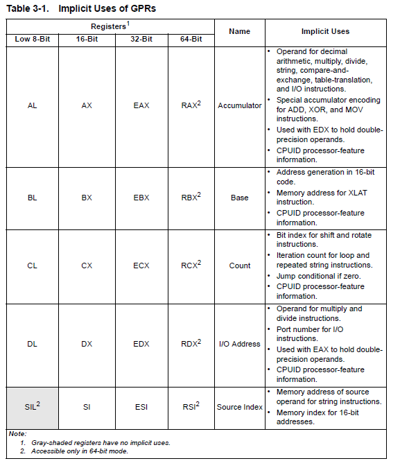
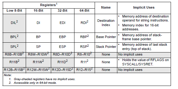
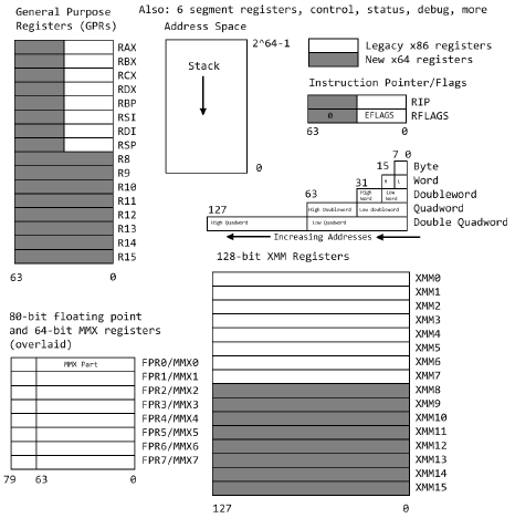
AX BX CX DX to store. Arithmetical registers
SP BP DI SI to access to memory
to address memory spaces
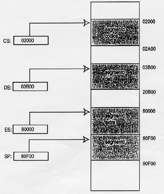
memory = Segments
address = Segment:Offset
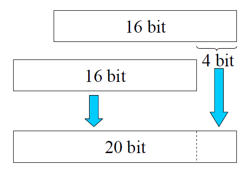
the segment = 16 bit + 0000 at right that multiply by 16)
eg : [CS] = 123Ah , [IP] = 341Bh
SEG:OFF = 123A0:341B = 123a0+341b=157BBh = physical address
from the top to bottom:
effective address
segment address
physical address
FLAGS are indicator bits (grouped into a status log named PSW register)
normally read by conditioned jump instructions
OF: overflow indicator. It is setted at 1 when the result of one
addition or subtraction (with sign ) causes overflow
SF: sign indicator. It is setted at 1 when the result of a logic-arithmetic
operation is a negative number (= MSB of the result)
ZF: zero indicator. It is setted at 1 when the result of a logic-arithmetic
operation is = zero
CF: setted at 1 when a logic-arithmetic operation gives a rest
(indicates overflow in case of numbers
without sign)
SIMD single instruction stream multiple data stream :
architecture in which different processing units processes multiple data streams in parallel.
This is used by vector processors or by processors that work in parallel.
SIMD is often used by supercomputers and with some variants even in modern microprocessors.
Threads refer to the highest level of code executed
by a processor, so with many threads, your CPU can
handle several tasks at the same time. All CPUs have
active threads, and every process performed on your
computer has at least a single thread.


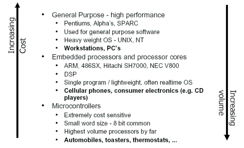
Unlike a microprocessor, the MICROCONTROLLER combines all the elements inside a single small container,
and in theory it does not need other external components to work.
Everything is in fact contained in a single chip, including the memory for the program, the RAM memory,
the clock oscillator, the reset circuit and the peripherals.
The calculation capabilities of a microcontroller are extremely small. For example the
RAM memory is made up of a few hundred cells, and is usually not expandable.
Among the typical applications of a
microcontroller there may be the burglar alarms, the measuring instruments,
those for brightness adjustment, battery chargers and transmitters / receivers.
For these reasons, microcontrollers are designed to run a small set of
specific functions, for example in the case of a Digital Signal Processor, which carries out a
small set of signal processing functions and is widely used for
adjust the brakes on all four wheels, or adjust the air conditioning in the car.
PIC
INTEL
16-bit Processors and Segmentation (1978)
The IA-32 architecture family was preceded by 16-bit processors, the 8086 and 8088.
The 8086 has 16-bit registers
and a 16-bit external data bus, with 20-bit addressing giving a 1-MByte address space.
The 8088 is similar to
the 8086 except it has an 8-bit external data bus.
The 8086/8088 introduced segmentation to the IA-32 architecture. With segmentation,
a 16-bit segment register
contains a pointer to a memory segment of up to 64 KBytes. Using four segment
registers at a time, 8086/8088
processors are able to address up to 256 KBytes without switching between segments.
The 20-bit addresses that
can be formed using a segment register and an additional 16-bit pointer provide
a total address range of 1 MByte.
The Intel 286 Processor (1982)
The Intel 286 processor introduced protected mode operation into the IA-32
architecture. Protected mode uses the
segment register content as selectors or pointers into descriptor tables.
Descriptors provide 24-bit base addresses
with a physical memory size of up to 16 MBytes, support for virtual memory
management on a segment swapping
basis, and a number of protection mechanisms. These mechanisms include:
• Segment limit checking
• Read-only and execute-only segment options
• Four privilege levels
The Intel386 Processor (1985)
The Intel386 processor was the first 32-bit processor in the IA-32 architecture family.
It introduced 32-bit registers
for use both to hold operands and for addressing. The lower half of each 32-bit Intel386
register retains the properties
of the 16-bit registers of earlier generations, permitting backward compatibility.
The processor also provides
a virtual-8086 mode that allows for even greater efficiency when executing programs
created for 8086/8088
processors.
In addition, the Intel386 processor has support for:
• A 32-bit address bus that supports up to 4-GBytes of physical memory
• A segmented-memory model and a flat memory model
• Paging, with a fixed 4-KByte page size providing a method for virtual memory management
• Support for parallel stages
The Intel486 Processor (1989)
The Intel486 processor added more parallel execution capability by expanding the
Intel386 processor’s instruction
decode and execution units into five pipelined stages. Each stage operates in parallel
with the others on up to
five instructions in different stages of execution.
In addition, the processor added:
• An 8-KByte on-chip first-level cache that increased the percent of instructions
that could execute at the scalar
rate of one per clock
• An integrated x87 FPU
• Power saving and system management capabilities
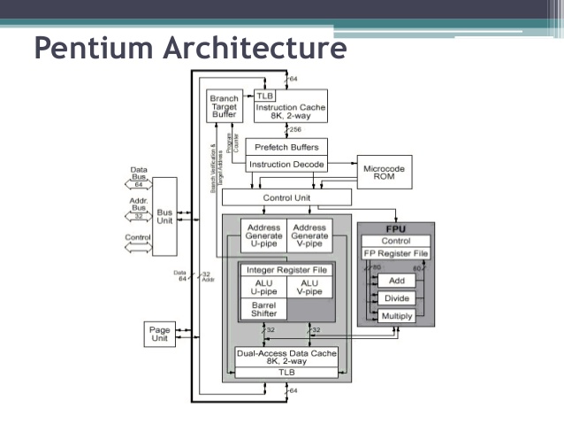
The Intel Pentium Processor (1993)
The introduction of the Intel Pentium processor added a second execution pipeline to achieve superscalar performance
(two pipelines, known as u and v, together can execute two instructions per clock). The on-chip first-level
cache doubled, with 8 KBytes devoted to code and another 8 KBytes devoted to data. The data cache uses the MESI
protocol to support more efficient write-back cache in addition to the write-through cache previously used by the
Intel486 processor. Branch prediction with an on-chip branch table was added to increase performance in looping
constructs.
In addition, the processor added:
• Extensions to make the virtual-8086 mode more efficient and allow for 4-MByte as well as 4-KByte pages
• Internal data paths of 128 and 256 bits add speed to internal data transfers
• Burstable external data bus was increased to 64 bits
• An APIC to support systems with multiple processors
• A dual processor mode to support glueless two processor systems
A subsequent stepping of the Pentium family introduced Intel MMX technology (the Pentium Processor with MMX
technology). Intel MMX technology uses the single-instruction, multiple-data (SIMD) execution model to perform
parallel computations on packed integer data contained in 64-bit registers.
See Section 2.2.7, “SIMD Instructions.”
2.1.6 The P6 Family of Processors (1995-1999)
The P6 family of processors was based on a superscalar microarchitecture that set new performance standards; see
also Section 2.2.1, “P6 Family Microarchitecture.” One of the goals in the design of the P6 family microarchitecture
was to exceed the performance of the Pentium processor significantly while using the same 0.6-micrometer, fourlayer,
metal BICMOS manufacturing process. Members of this family include the following:
• The Intel Pentium Pro processor is three-way superscalar. Using parallel processing techniques, the
processor is able on average to decode, dispatch, and complete execution of (retire) three instructions per
clock cycle. The Pentium Pro introduced the dynamic execution (micro-data flow analysis, out-of-order
execution, superior branch prediction, and speculative execution) in a superscalar implementation. The
processor was further enhanced by its caches. It has the same two on-chip 8-KByte 1st-Level caches as the
Pentium processor and an additional 256-KByte Level 2 cache in the same package as the processor.
• The Intel Pentium II processor added Intel MMX technology to the P6 family processors along with new
packaging and several hardware enhancements. The processor core is packaged in the single edge contact
cartridge (SECC). The Level l data and instruction caches were enlarged to 16 KBytes each, and Level 2 cache
sizes of 256 KBytes, 512 KBytes, and 1 MByte are supported. A half-frequency backside bus connects the Level
2 cache to the processor. Multiple low-power states such as AutoHALT, Stop-Grant, Sleep, and Deep Sleep are
supported to conserve power when idling.
• The Pentium II Xeon processor combined the premium characteristics of previous generations of Intel
processors. This includes: 4-way, 8-way (and up) scalability and a 2 MByte 2nd-Level cache running on a fullfrequency
backside bus.
INTEL 64 AND IA-32 ARCHITECTURES
• The Intel Celeron processor family focused on the value PC market segment. Its introduction offers an
integrated 128 KBytes of Level 2 cache and a plastic pin grid array (P.P.G.A.) form factor to lower system design
cost.
• The Intel Pentium III processor introduced the Streaming SIMD Extensions (SSE) to the IA-32 architecture.
SSE extensions expand the SIMD execution model introduced with the Intel MMX technology by providing a
new set of 128-bit registers and the ability to perform SIMD operations on packed single-precision floatingpoint
values. See Section 2.2.7, “SIMD Instructions.”
• The Pentium III Xeon processor extended the performance levels of the IA-32 processors with the
enhancement of a full-speed, on-die, and Advanced Transfer Cache.
The Intel Pentium 4 Processor Family (2000-2006)
The Intel Pentium 4 processor family is based on Intel NetBurst microarchitecture;
The Intel Pentium 4 processor introduced Streaming SIMD Extensions 2 (SSE2);
The Intel Pentium 4 processor 3.40 GHz, supporting Hyper-Threading Technology introduced Streaming
SIMD Extensions 3 (SSE3); see Section 2.2.7, “SIMD Instructions.”
Intel 64 architecture was introduced in the Intel Pentium 4 Processor Extreme Edition supporting Hyper-Threading
Technology and in the Intel Pentium 4 Processor 6xx and 5xx sequences.
Intel Virtualization Technology (Intel VT) was introduced in the Intel Pentium 4 processor 672 and 662.
Home Page